RV1126是瑞芯微推出的一款编解码芯片,专门面向人工智能的机器视觉领域,支持4K编码,支持8路1080P同编同解,内置独立NPU,支持人脸识别、骨骼识别、分析预警等,可广泛应用于智慧安防、视频通讯、视频分析等场景,目前在智能安防摄像头、视频会议摄像头、DMS系统、行车记录仪等产品均有项目落地。
1.1 Overview
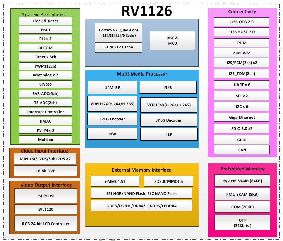
RV1126 is a high-performance vision processor SoC for IPC/CVR, especially for AI related application.It is based on quad-core ARM Cortex-A7 32-bit core which integrates NEON and FPU. There is a 32KB I-cache and 32KB D-cache for each core and 512KB unified L2 cache.The build-in NPU supports INT8/INT16 hybrid operation and computing power is up to 2.0TOPs. In addition, with its strong compatibility, network models based on a series of frameworks such as TensorFlow/MXNet/PyTorch/Caffe can be easily converted.
RV1126 also introduces a new generation totally hardware-based 14-megapixel ISP (image signal processor) and post processor. It implements a lot of algorithm accelerators usually used in IPC and CVR, such as HDR, 3A functions (AE, AF, AWB), LSC, 3DNR, 2DNR, sharpening, dehaze, fisheye correction, gamma correction, feature points detection and so on. All of them are real-time processing. Cooperating with two MIPI CSI (or LVDS/SubLVDS) and one DVP (BT.601/BT.656/BT.1120) interface, users can build a system that receives video data from 3 camera sensors simultaneous.
The video encoder embedded in RV1126 supports UHD H.265/H.264 encoding. It also supports multi-stream encoding, up to one 4Kp30 and one 1080p30 simultaneous. With the help of this feature, the video from camera can be encoded with higher resolution and stored in local memory and transferred another lower resolution video to cloud storage at the same time.The H.264/H.265 video decoder in RV1126 supports 4Kp30 for H.264 and H.265.
In addition to the previous high-performance multimedia block, RV1126 also contains rich audio, memory and other peripheral interfaces such as I2C, SPI, PWM and so on. These can help users add more sensors or other peripherals into whole system to improve flexibility and expansibility.
RV1126 has high-performance external DRAM (DDR3/DDR3L/DDR4/LPDDR3/LPDDR4-2133) capable of sustaining demanding memory bandwidths.
1.2 Features
The features listed below which may or may not be present in actual product, may be subject to the third-party licensing requirements. Please contact Rockchip for actual product feature configurations and licensing requirements.
1.2.1 Application Processor
Quad-Core Cortex-A7
Full implementation of the ARM architecture v7-A instruction set, ARM Neon Advanced SIMD
Separately Integrated Neon and FPU
32KB L1 I-Cache and 32KB L1 D-Cache per Cortex-A7 CPU
Unified 512KB L2 Cache for Quad-Core Cortex-A7
TrustZone technology supported
Separate power domains for CPU core system to support internal power switch and externally turn on/off based on different application scenario
PD_CPU0: 1st Cortex-A7 + Neon + FPU + L1 I/D Cache
PD_CPU1: 2nd Cortex-A7 + Neon + FPU + L1 I/D Cache
PD_CPU2: 3rd Cortex-A7 + Neon + FPU + L1 I/D Cache
PD_CPU3: 4th Cortex-A7 + Neon + FPU + L1 I/D Cache
One isolated voltage domain to support DVFS
1.2.2 Video Input Interface
Interface and video input processor
Two MIPI CSI/ LVDS/SubLVDS interfaces, 4 lanes each, MIPI CSI max data rate is 2.5Gbps/lane, LVDS/SublVDS max data rate is 1Gbps/lane
One 8/10/12/16-bit standard DVP interface, up to 150MHz input data
Support BT.601/BT.656 and BT.1120 VI interfaces
Support the polarity of pixel_clk、hsync、vsync configurable
RV1126 Datasheet Rev 1.4
ISP
Maximum resolution is 14Mpixel(4416×3312)
DVP input: ITU-R BT.601/656/1120 with raw8/raw10/raw12/raw16, YUV422
MIPI input: RX data lane x1/x2/x4, raw8/raw10/raw12, YUV422
3A: include AE/Histogram, AF, AWB statistics output
FPN: Fixed Pattern Noise removal
BLC: Black Level Correction
DPCC: Static/Dynamic defect pixel cluster correction
LSC: Lens shading correction
Bayer-NR: Bayer-raw De-noising, 2DNR
HDR: 3-/2-Frame Merge into High-Dynamic Range
TMO: 3-/2-Frame Merge Video Tone mapping
WDR: One Frame Wide-Dynamic Range Tone mapping
Debayer: Advanced Adaptive Demosaic with Chromatic Aberration Correction
CCM/CSM: Color correction matrix; RGB2YUV etc.
Gamma: Gamma out correction
Dehaze/Enhance: Automatic Dehaze and edge enhancement
3DLUT: 3D-Lut Color Palette for Customer
LDCH: Lens-distortion in the horizontal direction
Output Scale*3: support scale down level*3(W0<3264; W1<1280; W2<1280)
Output Scale*2: support scale down level*2(W0<1920; W1<1920)
Output (FBC): support YUV422/420 with Frame Buffer Compression
3DNR: Advanced Temporal Noise reduce in YUV
2DNR: Advanced Spatial Noise reduce in YUV
Sharp: Picture Sharpening & Edge Enhance in YUV
ORB: Oriented Fast and Rotated BRIEF, a method of feature points detection
FEC: the bigger Lens-distortion and Fish Eye Correction
CGC: Color Gamut Compression, YUV full range/limit range convert
1.2.3 Video CODEC
Video Decoder
Real-time decoding of H.264 and H.265
Main and Main10 profile for H.265, up to level 5.0 and 4096×2304@30fps
Baseline, main, high, high10 and high 4:2:2(without MBAFF), up to level 5.1 and 4096×2304@30fps
Video Encoder
Real-time UHD H.265/H.264 video encoding
I-/P-frames and SmartP reference.
Five bit rate control modes (CBR, VBR, FixQp, AVBR, and QpMap)
Up to 100 Mbit/s output bit rate
Support ROI(no limit) encoding;
High profile for H.264, up to level 5.1 and 4096×2304@30fps
Main profile for H.265, up to level 5.0 and 4096×2304@30fps
Support multi-stream encoding
3840 x 2160@30 fps + 1080p@30 fps encoding
3840 x 2160@30 encoding + 3840 x 2160@30 fps decoding
Input data format:
YCbCr 4:2:0 planar
YCbCr 4:2:0 semi-planar
YCbYCr 4:2:2
CbYCrY 4:2:2 interleaved
RGB444 and BGR444
RGB555 and BGR555
RGB565 and BGR565
RGB888 and BRG888
RGB101010 and BRG101010
RV1126 Datasheet Rev 1.4
One isolated voltage domain to support DVFS
1.2.4 JPEG CODEC
JPEG Encoder
Baseline (DCT sequential)
Encoder size is from 96×96 to 8192×8192(67Mpixels)
Up to 90 million pixels per second
JPEG Decoder
Decoder size is from 48×48 to 8176×8176(66.8Mpixels)
Up to 76 million pixels per second
1.2.5 Neural Process Unit
Neural network acceleration engine with processing performance up to 2.0 TOPS
Support integer 8, integer 16 convolution operation
Support deeplearning frameworks: TensorFlow, TF-lite, Pytorch, Caffe, ONNX, MXNet, Keras, Darknet
Support OpenVX API
One isolated voltage domain to support DVFS
1.2.6 Memory Organization
Internal on-chip memory
BootRom
SYSTEM_SRAM in the voltage domain of VD_LOGIC
PMU_SRAM in the voltage domain of VD_PMU for low power application
External off-chip memory
DDR3/DDR3L/DDR4/LPDDR3/LPDDR4-2133①
SPI Flash
eMMC
SD Card
Async Nand Flash
1.2.7 Internal Memory
Internal BootRom
Support system boot from the following device:
FSPI Flash interface
eMMC interface
SDMMC interface
Async Nand interface
Support system code download by the following interface:
USB OTG interface (Device mode)
SYSTEM_SRAM
Size: 64KB
PMU_SRAM
Size: 8KB
1.2.8 External Memory or Storage device
Dynamic Memory Interface (DDR3/DDR3L/DDR4/LPDDR3/LPDDR4-2133)
Compatible with JEDEC standards
Compatible with DDR3/DDR3L/DDR4/LPDDR3/LPDDR4-2133
Support 32-bit data width, 2 ranks (chip selects), max 4GB addressing space per rank, total addressing space is 4GB (max)
Low power modes, such as power-down and self-refresh for SDRAM
eMMC Interface
Compatible with standard iNAND interface
Compatible with eMMC specification 4.51
Support three data bus width: 1-bit, 4-bit or 8-bit
Support up to HS200; but not support CMD Queue
RV1126 Datasheet Rev 1.4
SD/MMC Interface
Compatible with SD3.0, MMC ver4.51
Data bus width is 4bits
Flexible Serial Flash Interface(FSPI)
Support transfer data from/to serial flash device
Support x1, x2, x4 data bits mode
Support 2 chips select
Nand Flash Interface
Support async nand flash
Data bus width is 8bits
Support 1 chip select
Support LBA nand flash
Up to 16bits/1KB hardware ECC
Support configurable interface timing
1.2.9 System Component
RISC-V MCU
32bit microcontroller core with RISC -V ISA
Harvard architecture, separate Instruction and Data memories
Instruction set is RV32I with M and C extensions
Integrated Programmable Interrupt Controller (IPIC), all 123 IRQ lines connected to GIC for Cortex-A7 also connect to RISC –V MCU
Integrated Debug Controller with JTAG interface
CRU (clock & reset unit)
Support clock gating control for individual components
One oscillator with 24MHz clock input
Support global soft-reset control for whole chip, also individual soft-reset for each component
PMU (power management unit)
Support 5 separate voltage domains VD_CORE/VD_LOGIC/VD_PMU/VD_NPU/VD_VEPU
Support 14 separate power domains, which can be power up/down by software based on different application scenes
Multiple configurable work modes to save power by different frequency or automatic clock gating control or power domain on/off control
Timer
Support 6 64bit-timers with interrupt-based operation for non-secure application
Support 2 64bit-timers with interrupt-based operation for secure application
Support two operation modes: free-running and user-defined count
Support timer work state checkable
PWM
Support 12 on-chip PWMs (PWM0~PWM11) with interrupt-based operation
Programmable pre-scaled operation to bus clock and then further scaled
Embedded 32-bit timer/counter facility
Support capture mode
Support continuous mode or one-shot mode
Provides reference mode and output various duty-cycle waveform
Optimized for IR application for PWM3, PWM7 and PWM11
Watchdog
32-bit watchdog counter
Counter counts down from a preset value to 0 to indicate the occurrence of a timeout
WDT can perform two types of operations when timeout occurs:
Generate a system reset
First generate an interrupt and if this is not cleared by the service routine by the time a second timeout occurs then generate a system reset
Programmable reset pulse length
RV1126 Datasheet Rev 1.4
Totally 16 defined-ranges of main timeout period
One Watchdog for non-secure application
One Watchdog for secure application
Interrupt Controller
Support 128 SPI interrupt sources input from different components
Support 16 software-triggered interrupts
Two interrupt outputs (nFIQ and nIRQ) separately for each Cortex-A7, both are low-level sensitive
Support different interrupt priority for each interrupt source, and they are always software-programmable
DMAC
Micro-code programming-based DMA
Linked list DMA function is supported to complete scatter-gather transfer
Support data transfer types with memory-to-memory, memory-to-peripheral, peripheral-to-memory
Signals the occurrence of various DMA events using the interrupt output signals
One embedded DMA controller for system
DMAC features:
Support 8 channels
27 hardware requests from peripherals
2 interrupts output
Support TrustZone technology and programmable secure state for each DMA channel
Secure System
Cipher engine
Support SM2/SM3/SM4 cipher
Support SHA-1, SHA-256/224, SHA-512/384, MD5 with hardware padding
Support Link List Item (LLI) DMA transfer
Support AES-128 AES-256 encrypt & decrypt cipher
Support AES ECB/CBC/OFB/CFB/CTR/CTS/XTS mode
Support DES & TDES encrypt & decrypt cipher
Support DES/TDES ECB/CBC/OFB/CFB mode
Support up to 4096 bits PKA mathematical operations for RSA/ECC
Support up to 8-channels configuration
Support Up to 256 bits TRNG output
Support data scrambling for all DDR types
Support secure OTP
Support secure debug
Support secure OS
Mailbox
One Mailbox in SoC to service A7 and RISC-V MCU communication
Support four mailbox elements per mailbox, each element includes one data word, one command word register and one flag bit that can represent one interrupt
Provide 32 lock registers for software to use to indicate whether mailbox is occupied
DECOM
Support for decompressing GZIP files
Support for decompressing LZ4 files, including the General Structure of LZ4 Frame format and the Legacy Frame format.
Support for decompressing data in Deflate format
Support for decompressing data in ZLIB format
Support complete interrupt and error interrupt output
Support Hash32 check in LZ4 decompression process
Support the limit size function of the decompressed data to prevent the memory from being maliciously destroyed during the decompression process
Support software to stop the decompression process
RV1126 Datasheet Rev 1.4
1.2.10 Graphic Engine
2D Graphics Engine (RGA):
Source formats:
ABGR8888, XBGR888, ARGB8888, XRGB888
RGB888, RGB565
RGBA5551, RGBA4444
YUV420 planar, YUV420 semi-planar
YUV422 planar, YUV422 semi-planar
YUV 10-bit for YUV420/422 semi-planar
BPP8, BPP4, BPP2, BPP1
Destination formats:
ABGR8888, XBGR888, ARGB8888, XRGB888
RGB888, RGB565
RGBA5551, RGBA4444
YUV420 planar, YUV420 semi-planar
YUV422 planar, YUV422 semi-planar
Pixel Format conversion, BT.601/BT.709
Max resolution: 8192×8192 source, 4096×4096 destination
BitBLT
Two source BitBLT:
A+B=B only BitBLT, A support rotate and scale when B fixed
A+B=C second source (B) has same attribute with (C) plus rotation function
Color fill with gradient fill, and pattern fill
High-performance stretch and shrink
Monochrome expansion for text rendering
New comprehensive per-pixel alpha (color/alpha channel separately)
Alpha blending modes including Java 2 Porter-Duff compositing blending rules, chroma key, pattern mask, fading
Dither operation
0, 90, 180, 270-degree rotation
x-mirror, y-mirror and rotation operation
Image Enhancement Processor (IEP):
Image format
Input data: YUV420/YUV422, semi-planar/planar, UV swap
Output data: YUV420/YUV422, semi-planar, UV swap, Tile mode
YUV down sampling conversion from 422 to 420
Max resolution for dynamic image up to 1920×1080
De-interlace
1.2.11 Display Interface
One up to 24 bits RGB parallel video output interface
One BT.1120 video output interface
One 4 lane MIPI DSI interface, up to 1Gbps per lane
Up to 1080p@60fps
1.2.12 Video Output Processor (VOP)
Up to 1920×1080 @60fps
Multiple layer
Background layer
Win0 layer
Win2 layer
Input format: RGB888, ARGB888, RGB565, YCbCr422, YCbCr420, YCbCr444
1/8 to 8 scaling-down and scaling-up engine
Support virtual display
256 level alpha blending (pre-multiplied alpha support)
Transparency color key
RV1126 Datasheet Rev 1.4
YCbCr2RGB (rec601-mpeg/ rec601-jpeg/rec709)
RGB2YCbCr (BT.601/BT.709)
Support multi-region
Win0 layer and Win2 layer overlay exchangeable
Support RGB or YUV domain overlay
BCSH (Brightness, Contrast, Saturation, Hue adjustment)
BCSH: YCbCr2RGB (rec601-mpeg/ rec601-jpeg/rec709)
BCSH: RGB2YCbCr (BT.601/BT.709)
Support Gamma adjust
Support dither down allegro RGB888to666 RGB888to565 & dither down FRC (configurable) RGB888to666
Blank and black display
1.2.13 Audio Interface
I2S0 with 8 channels
Up to 8 channels TX and 8 channels RX path
Audio resolution from 16bits to 32bits
Sample rate up to 192KHz
Provides master and slave work mode, software configurable
Support 3 I2S formats (normal, left-justified, right-justified)
Support 4 PCM formats (early, late1, late2, late3)
I2S and PCM mode cannot be used at the same time
I2S1/I2S2 with 2 channels
Up to 2 channels for TX and 2 channels RX path
Audio resolution from 16bits to 32bits
Sample rate up to 192KHz
Provides master and slave work mode, software configurable
Support 3 I2S formats (normal, left-justified, right-justified)
Support 4 PCM formats (early, late1, late2, late3)
I2S and PCM cannot be used at the same time
PDM
Up to 8 channels
Audio resolution from 16bits to 24bits
Sample rate up to 192KHz
Support PDM master receive mode
TDM
Support up to 8 channels for TX and 8 channels RX path
Audio resolution from 16bits to 32bits
Sample rate up to 192KHz
Provides master and slave work mode, software configurable
Support 3 I2S formats (normal, left-justified, right-justified)
Support 4 PCM formats (early, late1, late2, late3)
Audio PWM
Support convert PCM to PWM format
Sample rate up to 16x
Support linear interpolation for 2x/4x/8x/16 oversampling
Support 8/9/10/11 bits maskable L/R channel PWM output
Digital Audio Codec
Support 3-channel digital ADC
Support 2-channel digital DAC
Support I2S/PCM interface
Support I2S/PCM master and slave mode
Support 4-channel audio transmitting in I2S mode
Support 2-channel audio receiving in I2S mode
Support 2-channel audio transmitting or receiving in PCM mode
Support 16~24 bit sample resolution for both digital ADC and digital DAC
RV1126 Datasheet Rev 1.4
Both digital ADC and digital DAC support three groups of sample rates. Group 0 are 8khz/16khz/32kHz/64kHz/128khz, group 1 are 11.025khz/22.05khz/44.1khz/88.2khz/176.4khz and group 2 are 12khz/24khz/48khz/96khz/192khz
The passband of digital ADC filters is 0.45625*fs
Support digital ADC pass-band ripple within +/-0.1dB
The stop-band of digital ADC filters is 0.5*fs
Support digital ADC stop-band attenuation at least 60dB
Support volume control for both digital ADC and digital DAC
Support Automatic Level Control (ALC)and noise gate for digital ADC
Support communication with Analog Codec through I2C bus
1.2.14 Connectivity
SDIO Interface
Compatible with SDIO3.0 protocol
4bits data bus widths
GMAC 10/100/1000M ethernet controller
Support 10/100/1000-Mbps data transfer rates with the RGMII interfaces
Support 10/100-Mbps data transfer rates with the RMII interfaces
Support both full-duplex and half-duplex operation Support for TCP Segmentation Offload (TSO) and UDP Segmentation Offload (USO) network acceleration
USB 2.0 Host
Compatible with USB 2.0 specification
Supports high-speed(480Mbps), full-speed(12Mbps) and low-speed(1.5Mbps) mode
Support Enhanced Host Controller Interface Specification (EHCI), Revision 1.0
Support Open Host Controller Interface Specification (OHCI), Revision 1.0a
USB 2.0 OTG
Compatible Specification
Universal Serial Bus Specification, Revision 2.0
Extensible Host Controller Interface for Universal Serial Bus (xHCI), Revision 1.1
Support Control/Bulk/Interrupt/Isochronous Transfer
SPI Interface
Support 2 SPI Controllers, support two chip-select output
Support serial-master and serial-slave mode, software-configurable
I2C Interface
Support 6 I2C interfaces(I2C0-I2C5)
Support 7bits and 10bits address mode
Software programmable clock frequency
Data on the I2C-bus can be transferred at rates of up to 100k bits/s in the Standard-mode, up to 400k bits/s in the Fast-mode or up to 1m bits/s in Fast-mode Plus
UART Interface
Support 6 UART interfaces (UART0-UART5)
Support 5bit, 6bit, 7bit, 8bit serial data transmit or receive
Standard asynchronous communication bits such as start, stop and parity
Support different input clock for UART operation to get up to 4Mbps baud rate
Support auto flow control mode(except UART2)
1.2.15 Others
Multiple Groups of GPIO
All of GPIOs can be used to generate interrupt
Support level trigger and edge trigger interrupt
Support configurable polarity of level trigger interrupt
Support configurable rising edge, falling edge and both edge trigger interrupt
Support configurable pull direction (a weak pull-up and a weak pull-down)
RV1126 Datasheet Rev 1.4
Support configurable drive strength
Temperature Sensor (TS-ADC)
Support User-Defined Mode and Automatic Mode
In User-Defined Mode, start_of_conversion can be controlled completely by software, and also can be generated by hardware.
In Automatic Mode, the temperature of alarm(high/low temperature) interrupt can be configurable
In Automatic Mode, the temperature of system reset can be configurable
Support to 2 channel TS-ADC (used for CPU and NPU respectively), the temperature criteria of each channel can be configurable
-40~125°C temperature range and 5°C temperature resolution
12-bit SARADC up to 732 S/s sampling rate
Successive approximation ADC (SARADC)
10-bit resolution
Up to 1MS/s sampling rate
6 single-ended input channels
OTP
Support 32Kbit space and higher 4k address space is non-secure part.
Support read and program word mask in secure model
Support program length from 1 to 32 bit
Read operation support 8bit only
Program and Read state can be read
Program fail address record
Package type
FCCSP 409-pin (body: 14mm x 14mm; ball size: 0.3mm; ball pitch: 0.65mm)
Notes:
① : DDR3/DDR3L/DDR4/LPDDR3/LPDDR4 are not used simultaneously
RV1126 Datasheet Rev 1.4