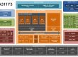
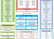
 RK1608是一款低功耗、高性能DSP的视觉处理通用型SoC。可应用于智能手机中的3DNR、EIS、HDR等,也可用于人脸识别模块等机器视觉领域。现有RK1608B、RK1608B2、RK1608A1、RK1608A2 4种型号,主要与嵌入式DRAM的容量不同。下面为RK1608的芯片简介Datasheet。
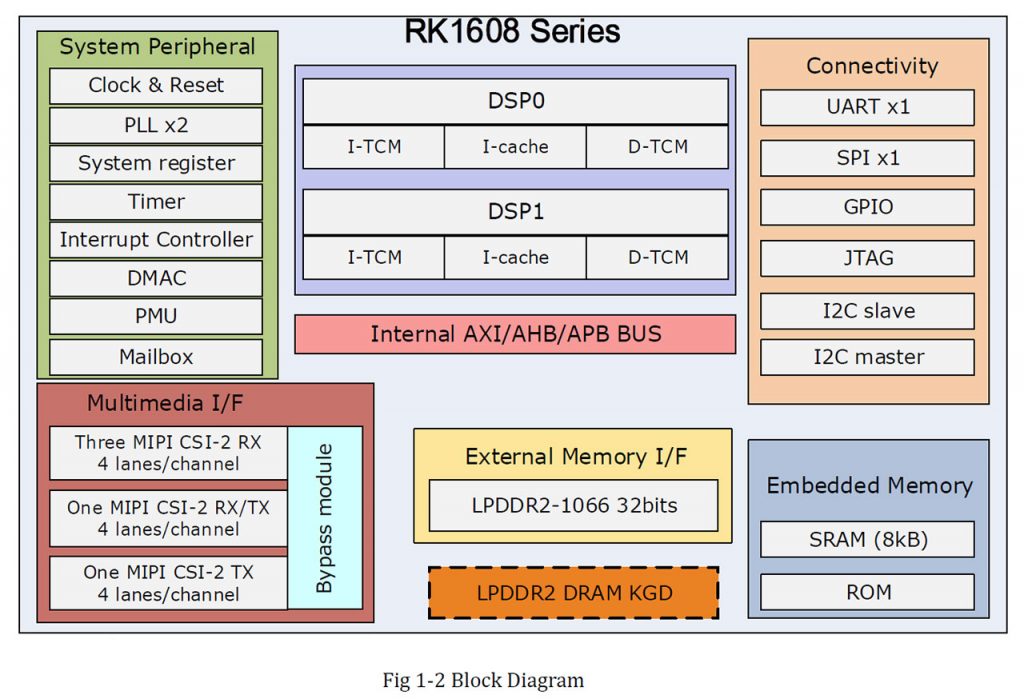
1.2.1 DSP core
- Dual-core DSP
- 2 separate power domains for system to support internal power switch and externally turn on/off based on different application scenario
- PD_DSP0: DSP0 + L1 I Cache, I/D-TCM
- PD_DSP1: DSP1 + L1 I Cache, I/D-TCM
1.2.2 Memory Organization
- Internal on-chip memory
- Boot Rom
- SRAM
- LPDDR2
1.2.3 Internal Memory
- Internal Boot Rom
- Support system boot from the following device:
- SPI NOR flash
- SPI slave interface
- Internal SRAM
- Size: 8KB
- Support system boot from the following device:
- Internal DRAM
- RK1608B: LPDDR2-1066, 2Gb KGD
- RK1608B2: LPDDR2-1066, 2Gb KGD
- RK1608A1: LPDDR2-1066, 1Gb KGD
- RK1608A2: LPDDR2-1066, 1Gb KGD
1.2.4 System Component
- CRU (clock & reset unit)
- Support clock gating control for individual components
- One oscillator is for clock input and 2 embedded PLLs
- Support global soft-reset control for whole SoC, also individual soft-reset for every component
- PMU (power management unit)
- Multiple configurable work modes to save power by different frequency or automatically clock gating control or power domain on/off control
- Lots of wakeup sources in different mode
- 2 separate voltage domains
- 2 separate power domains for two DSP cores, which can be powered up/down by software based on different application scenes
- Bus Architecture
- 128-bit/64-bit/32-bit AXI/AHB/APB composite bus architecture
- 1 embedded AXI interconnect
- For the interconnect with AXI/AHB/APB composite bus, clocks for AXI/AHB/APB domains are always synchronous, and different integer ratio is supported for
- Flexible different QoS solution to improve the utility of bus bandwidth
- Interrupt Controller
- Support 3 interrupt controllers for two DSPs and AP
- Support 64 SPI interrupt sources input from different components
- Support different interrupt priority for each interrupt source, and they are always software-programmable
- DMA Controller
- Support AMBA 2.0 AHB slave interface for accessing internal registers and LUT memories,32bit data bus width
- Support AMBA 3.0 AXI master read interface for loading frame data
- There is a high-level indicated interrupt signal for each channel
- DMA channels are based on chain table
- Support 2-D transmission, 3 type of DMA operation mode:
- Normal mode, the data is being transferred without change
- 10-bit compact RAW mode: data from RAW10 will be reordered to be continuous 10-bit data, each pixel will only occupy 10 bits storage space in memory
- 10-bit redundant RAW mode: data from RAW10 will be reordered to be continuous 10 bits data, each pixel will only occupy 16 bits storage space in memory, the upper 6 bits or the little 6 bits will be padding with 0
- Target address alignment:
- Normal mode, byte alignment is supported
- 10-bit compact RAW mode: destination address may be byte alignment; source address need to be 2-byte alignment
- 10-bit redundant RAW mode: destination address need to be 2-byte alignment, source address may be byte alignment and the valid data may be configured from bit 0/2/4/6 in the 16 bits storage unit
- Only support software program it, not from peripheral
- Timer
- One 64-bit Timer in SoC with interrupt-based operation for application
- Provide two operation modes: free-running and user-defined count
- Support timer work state checkable
- MailBox
- One MailBox in SoC to serve communication between two DSP cores or between DSP core and AP
- Support four elements per mailbox, each element includes one data word, one command word register and one flag bit that can represent one interrupt
- Provide 32 lock registers for software to use to indicate whether mailbox is occupied
1.2.5 Video IN/OUT
- VIP (Video Input Processor)
- Support sampling image RAW data and PDAF data
- Support raw 8/10 bit
- Support reordering the sampling data or not reordering
- Support 1/4、1/16、1/64、1/256 scaling in the gray domain and RGB domain
- Support combined interrupt output
- Support ping-pong mode
- Support virtual line
- Support debug mode
- VOP (Video Output Processor)
- Display interface
- Parallel RGB Interface
- Display interface
² RAW8/10
- Parallel PDAF Interface
² RAW8/10
- Support IDI interface
- Layer process
- Background layer
- programmable RAW10 data
- Win layer – win0
- Support data format
- RAW8/RAW10
- Support virtual display
- Support display offset
- Master Address 64-bit aligned
- Stride 64-bit aligned
- Support data format
- Bus interface
- Support AMBA 2.0 AHB slave interface for accessing internal registers and LUT memories,32bit data bus width
- Support AMBA 3.0 AXI master read interface for loading frame data
- 64-bit data bus width
- Support NOC hurry for higher bus priority for win0
- Support bypass path from Rx to Tx
- Background layer
1.2.6 MIPI CSI-2 Transmitter Controller
CSI-2 Transmitter Features
- Compliant with MIPI CSI-2 v1.3 specification
- CSI2 TX lane configuration: Programmable 1, 2 or 4 Data Lane Configuration
- Operate in continuous clock mode
- Supported YUV Data Types: YUV420_8bit, YUV420_10bit, YUV422_8Bit, YUV422_10bit, YUV420_8Bit_CSPS, YUV420_10bit_CSPS and LEGACYYUV420_8bit
- Supported RGB Data Types: RGB888, RGB565, RGB666, RGB555, and RGB444
- Supported RAW Data Types: RAW8, RAW10
- Supported User defined (8-bit) Data Types
- Camera Interface: 8, 16 and 24 bit per pixel
- Data rate: CSI-2 with DPHY: up to 1.5Gbps per lane
- Supports VC interleaving
1.2.7 MIPI CSI-2 Receiver Controller
- The CSI-2 Host Controller implements the CSI-2 protocol on the host side
- Compliant with MIPI Alliance Specification for CSI-2, Version 01
- Dynamically configurable multi-lane merging
- Long and Short packet decoding
- Timing accurate signaling of Frame and Line synchronization packets
- 32-bit Image Data Interface delivering data formatted as recommended in CSI-2 Specification
- Support Frame formats
- General Frame or Digital Interlaced Video with or without accurate sync timing
- Data Type (Packet or Frame Level) and Virtual Channel interleaving
- Support data formats
- RGB, YUV, and RAW color space definitions
- From 24-bit down to 6-bit per pixel
- Generic or user-defined byte-based data types
- Error detection and correction
1.2.8 MIPI D-PHY
- Compliant with the MIPI D-PHY interface specification, revision 1
- There are totally 5 MIPI D-PHY for RK1608B
- Flexible input clock reference – 5MHz to 500MHz
- 50% DDR output clock duty-cycle
- Embedded 1 MIPI_CSI TX PHY
- Support 4 data lanes in this PHY
- Providing up to 1.5Gbps data rate per lane
- Embedded 3 MIPI_CSI RX PHY
- Support 4 data lanes per RX PHY
- Providing up to 1.5Gbps data rate per lane
- Embedded 1 MIPI_CSI TX and RX Combo PHY
- The PHY can be configured as TX or RX. TX and RX could not work
- Support 4 data lanes in this PHY
- Providing up to 1.5Gbps data rate per lane
1.2.9 Connectivity
- SPI Controller
- One on-chip SPI controller
- Support serial-master and serial-slave mode, software-configurable
- DMA-based or interrupt-based operation
- Embedded two 32x16bits FIFO for TX and RX operation respectively
- Support 1 chip-select output in serial-master mode
- UART Controller
- 1 on-chip UART interface
- DMA-based or interrupt-based operation
- For all UART, two 64Bytes FIFOs are embedded for TX/RX operation respectively
- Support 5bit,6bit,7bit,8bit serial data transmit or receive
- Standard asynchronous communication bits such as start, stop and parity
- Support different input clock for UART operation to get up to 4Mbps or other special baud rate
- Support non-integer clock divides for baud clock generation
- Auto flow control mode is for all UART, except UART_DBG
- I2C interface
- Compliant with I2C bus Specification, Version 0. But high-speed mode is not supported.
- Data on the I2C-bus can be transferred at rates of up to 100 kbps in the Standard- mode, up to 400 kbps in the Fast-mode or up to 1 Mbit/s in Fast-mode Plus mode
- Four I2C master controllers and one I2C slave controller
- Support 7-bit and 10-bit address mode
- Software programmable clock frequency and transfer rate
- GPIO
- All of GPIOs can be used to generate interrupt to DSP
- The pull direction (pullup or pulldown) for all of GPIOs are software-programmable
- All of GPIOs are always in input direction in default after power-on-reset
- The drive strength for all of GPIOs is software-programmable
Notes:
① Actual maximum frame rate will depend on the clock frequency and system bus performance
② Actual maximum data rate will depend on the clock frequency